01Si
SiliconOpaque. Rigid. Heat intensive.
Wafer silicon is proven and durable, but its conventional format cannot turn a transparent window into a generating surface.
Integration limits
Antimony chalcogenide thin films, engineered for the surfaces around us.
Explore the material

Wafer silicon is proven and durable, but its conventional format cannot turn a transparent window into a generating surface.
Integration limitsA successful thin-film technology built around scarce tellurium and a cadmium-containing absorber. Supply and end-of-life recovery matter.
Scarcity + material safetyFour-element composition requires tight process control. Indium and gallium supply is concentrated in China, creating geopolitical exposure.
Composition + critical mineralsHeat, moisture and light can destabilise the absorber; mobile ions add another degradation pathway. Lead creates a separate containment challenge.
Stability + leadLead-halide perovskites face fundamental chemical and ionic stability challenges. Encapsulation protects a device; it does not remove the absorber’s underlying degradation mechanisms.
Our platform starts with an intrinsically stable, inorganic antimony chalcogenide absorber. Device design and encapsulation then build on that foundation.

Absorb energy.
Let light through.
Very high visible-light absorption lets an exceptionally thin film capture energy.
Reported absorption coefficientReducing absorber thickness lets more light pass through. Thickness, composition and electrodes shape transparency.
A tunable optical balanceOriented crystal ribbons can span the film thickness, giving carriers direct pathways with benign grain boundaries.
Single-crystal-like transport pathsSb₂S₃ and Sb₂Se₃ offer simple chemistry. Their ribbon structure can tolerate grain boundaries.
Alloyed as Sb₂(S,Se)₃Lead exposure can cause irreversible neurological harm, especially in children. Lead-containing absorbers require containment and recovery.
WHO · Lead exposureCadmium can damage kidneys, bones and the respiratory system. It is a human carcinogen; exposure prevention and end-of-life control are essential.
WHO · Cadmium exposureAntimony chalcogenide provides a lower-toxicity absorber pathway without Pb or Cd in its composition.
Sb₂(S,Se)₃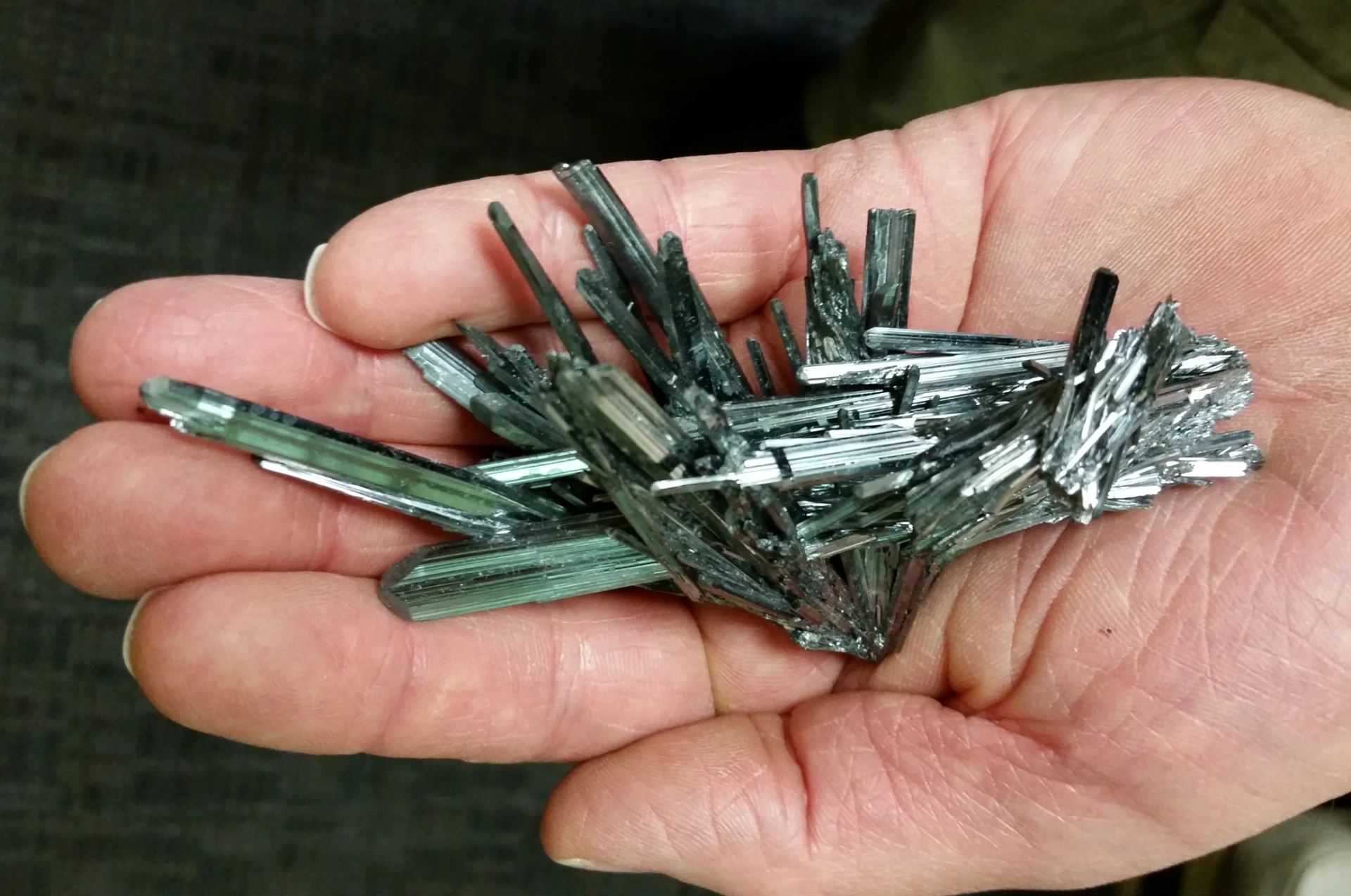
Antimony occurs naturally in stibnite. Australian production offers a local starting point for a resilient supply pathway, with refined precursors engineered into our thin-film absorber. Our platform avoids the tellurium used in CdTe and the gallium used in CIGS — pairing small material demand with an Australian route to scale.
of one Australian mine’s 2024 antimony output
for 1 GW of modules.
Illustrative material calculation: 200 nm absorber, 10% module efficiency and 0.65 g antimony/m².
Mine production source · 2024Antimony is approximately 200 times more abundant than tellurium in Earth’s crust.
Crustal abundance, not a measure of refined supply.
Primary production
Used in CIGS absorbersRefined production
Used in CIGS absorbersRefined production
Used in CdTe absorbersChanging the sulphur-to-selenium ratio tunes the bandgap across approximately 1.1–1.7 eV. Film thickness and the device stack then determine the balance between light absorption and transmission.
That flexibility opens a route to semitransparent, bifacial and tandem devices.
Read the optical researchApproximate cutoff · 886 nm
Vacuum deposition and high-temperature stages are common in established solar manufacturing, adding equipment and energy demands.
Grow the light-harvesting layer from a chemical solution, using a low-temperature hydrothermal route rather than vacuum absorber deposition.
Chen Qian and colleagues improve hydrothermal growth, achieving 11.02% measured and 10.7% certified efficiency.
Advanced Materials · 2023Chen Qian and colleagues demonstrate light collection from both sides.
Journal of Materials Chemistry A · 2022Chen Qian and colleagues demonstrate all-inorganic Sb₂(S,Se)₃ solar cells using an MnS hole-transport layer.
Turning materials research into a technology platform for integration and licensing.
Discuss a technology partnershipPlease rotate your phone
to portrait